
Beauty Tools & Accessories
Print Flexible PCBs With A 3D Printer
Jul
Printing flexible PCBs with a 3D printer sounds like the kind of project that begins with optimism, caffeine, and one suspicious roll of filament. The good news? It is possible to make flexible circuit prototypes using 3D printing techniques. The slightly less glamorous news? It is not always as simple as pressing “print” and watching a finished bendy circuit board roll off the build plate like a tiny electronic fruit leather.
Still, the idea is exciting for makers, engineers, students, hardware startups, and anyone who has ever waited too long for a PCB order and thought, “There has to be a faster way.” Flexible printed circuit boards, or flex PCBs, are used in wearables, sensors, medical devices, foldable gadgets, cameras, automotive electronics, and compact consumer products where a rigid board would be about as useful as a brick in a smartwatch.
Thanks to additive manufacturing, conductive inks, flexible substrates, and creative maker workflows, 3D printers can now help produce flexible circuits in several practical ways. Some methods use a 3D printer to apply an etch-resistant pattern onto copper-clad flexible material. Others use conductive ink on PET or polyimide film. More advanced systems use direct ink writing to dispense silver inks, dielectric materials, gels, pastes, and even multilayer electronic structures. This guide explains how the process works, what materials are involved, where the limitations hide, and how to approach the project without turning your workbench into a tiny chemistry crime scene.
What Is a Flexible PCB?
A flexible PCB is a printed circuit board built on a bendable substrate instead of a rigid fiberglass board. Traditional rigid PCBs usually use FR-4, a stiff glass-reinforced epoxy laminate. Flexible PCBs often use polyimide, PET, Kapton-style films, polyester, or other thin polymer materials that can bend, fold, or conform to tight spaces.
The “flexible” part is not just a party trick. Flex circuits reduce wiring, save space, lower weight, and allow electronics to fit into products with curves, hinges, moving parts, or body-worn surfaces. A fitness tracker, camera ribbon cable, medical patch, foldable display, or compact drone assembly may use flexible circuitry because it can snake through places where a rigid PCB would simply refuse to cooperate.
Flexible PCB vs. Printed Flexible Electronics
It helps to separate two related ideas. A conventional flexible PCB usually has copper traces laminated onto a flexible substrate and manufactured with professional PCB processes. Printed flexible electronics, on the other hand, may use conductive inks printed directly onto a film. In the middle sits flexible hybrid electronics, where printed traces are combined with conventional components such as chips, resistors, LEDs, sensors, and connectors.
When people say they want to print flexible PCBs with a 3D printer, they may mean one of three things: using a printer as an etch-resist tool, printing conductive material directly, or using professional additive electronics equipment. All three are real. All three have trade-offs. None of them will magically replace every PCB factory by Tuesday.
Can You Really Print Flexible PCBs With a 3D Printer?
Yes, but the answer depends on your definition of “print.” A normal desktop FDM printer is not usually printing a complete high-performance PCB in one step. Instead, it can help create the pattern, mask, mold, channel, fixture, stencil, or experimental conductive path needed to make a working flexible circuit.
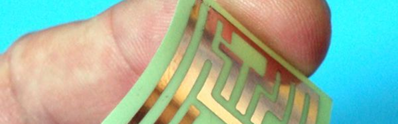
For example, one maker-friendly method involves printing a flexible filament such as NinjaFlex onto thin copper or conductive fabric. The printed plastic acts as an etch resist. After etching away the exposed copper, the remaining copper becomes the circuit trace. In this approach, the 3D printer is not printing copper; it is printing the protective pattern that lets you shape copper chemically.
Another path uses conductive ink. Specialized electronics printers can dispense silver-based ink onto PET, polyimide, or other flexible films. After curing or sintering, the ink becomes a conductive path. This is closer to what people imagine when they hear “printed circuit.” It is also where equipment, material compatibility, surface preparation, and curing temperature become much more important.
A third option uses conductive filament. Carbon-filled PLA or other conductive thermoplastics can be printed on a desktop 3D printer, but these materials usually have much higher resistance than copper. That makes them useful for touch sensors, resistors, low-current experiments, capacitive buttons, and educational prototypes, but less suitable for dense, high-speed, power-hungry circuit boards.
Why Use a 3D Printer for Flexible PCB Prototyping?
The biggest advantage is speed. Instead of waiting days or weeks for a prototype flex board, a designer can test a routing idea, sensor layout, LED strip, wearable patch, connector geometry, or enclosure-integrated circuit in-house. For early-stage product development, that can save money and keep the creative momentum alive.
Another advantage is customization. A 3D printer lets you experiment with unusual shapes, curved layouts, embedded channels, strain-relief features, custom fixtures, and flexible circuits that conform to a product instead of forcing the product to conform to the circuit. This matters in wearable electronics, robotics, prosthetics, soft sensors, smart textiles, compact IoT devices, and medical prototypes.
There is also less waste in additive processes. Traditional subtractive PCB manufacturing removes unwanted copper from a larger sheet. Printing conductive material only where needed can reduce material waste, especially when working with expensive silver inks. That said, chemical etching still involves safety and disposal responsibilities, so “DIY” should never mean “pour mystery liquid down the sink and hope the plumbing forgives you.”
Main Methods for Printing Flexible PCBs With a 3D Printer
1. Printing an Etch Resist on Flexible Copper
This is one of the most accessible methods for makers. The workflow starts with thin copper-clad flexible material or conductive fabric. A 3D printer lays down a pattern using flexible filament or another plastic that adheres to copper. That pattern protects selected copper areas during etching. After etching, the unwanted copper is removed, leaving behind the traces.
The benefit is that the final conductor is real copper, which has much better conductivity than most printable conductive filaments. The downside is that you still need an etching process, careful alignment, good bed leveling, and safe chemical handling. The first layer height is critical because the filament must bond to the copper without smearing, skipping, or becoming modern art.
2. Direct Ink Writing With Conductive Ink
Direct ink writing uses a controlled dispensing system to deposit conductive inks onto a substrate. In flexible electronics, silver ink is common because it offers strong conductivity compared with many printable alternatives. The substrate might be PET film, polyimide, TPU, paper, or another flexible material, depending on the ink and curing requirements.
This method is powerful because it can support fast iteration without screens, stencils, or masks. Engineers can change a design, print another version, test it, and repeat. Some professional systems can handle a wide range of viscosities, support multilayer printing, and print on rigid, compliant, or unconventional substrates. For research and development, this is where 3D printing starts to feel less like a hack and more like a manufacturing strategy.
3. Conductive Filament Printing
Conductive PLA, conductive TPU, and other filled thermoplastic filaments can create simple electrical paths. These materials often contain carbon black, graphene, copper particles, or other conductive fillers. They are easy to print compared with liquid ink systems, but they are not copper replacements.
Many conductive filaments behave more like resistors than wires. A short length may measure hundreds or thousands of ohms depending on the material, geometry, print settings, layer bonding, and direction of current flow. That makes conductive filament useful for touch pads, simple sensors, low-current LED demonstrations, or resistance-based components. It is usually a poor choice for fine-pitch microcontroller routing, high-current power rails, RF design, or anything where signal integrity matters.
4. 3D Printed Channels Filled With Conductive Material
Another creative method is to print a flexible or semi-flexible substrate with shallow channels, then fill those channels with conductive ink, silver paste, copper paint, or another conductive medium. The 3D print becomes the mechanical structure, and the conductive material forms the circuit.
This approach can be useful for prototypes, especially when the circuit needs to wrap around a curved object. However, it requires careful control over channel width, ink viscosity, curing, adhesion, and resistance. If the channels are too shallow, the trace may break. If they are too deep, filling them neatly becomes a miniature plumbing project.
5. Hybrid Printed Electronics
Hybrid printed electronics combine printed traces with conventional components. For example, a flexible substrate may carry printed silver traces, while LEDs, sensors, microcontrollers, and connectors are attached using conductive epoxy, low-temperature solder, anisotropic conductive film, Z-axis tape, crimp connectors, or mechanical interconnects.
This is often the most practical route for real devices. Fully printed transistors, resistors, capacitors, and antennas are possible in research and specialized manufacturing, but most functional prototypes still rely on conventional components. The magic is in connecting those components to a flexible printed circuit reliably.
Materials You Need
Flexible Substrates
Common substrate choices include PET, polyimide, Kapton-style film, polyester, TPU, flexible copper-clad laminate, and conductive fabric. PET is affordable and works well for many low-temperature printed electronics projects. Polyimide handles higher temperatures and is widely used in professional flex circuits. TPU and silicone-like materials are useful for stretchable applications, but they can be harder to print on because adhesion and curing become more challenging.
Conductive Materials
Copper is still the king for conductivity. If your method leaves actual copper traces, performance will usually be much better than carbon-filled plastic. Silver conductive ink is popular in printed electronics because it prints well and conducts reasonably after curing. Carbon inks are less conductive but useful for resistive sensors, touch interfaces, and cost-sensitive designs. Liquid metal inks are promising for stretchable circuits, though they are not yet as common in home workshops.
Insulating and Protective Layers
A flexible PCB needs protection. In professional boards, a coverlay insulates traces and improves durability. In DIY work, people may use flexible coatings, Kapton tape, UV-curable solder mask, silicone, polyurethane, or printed dielectric layers. The protective layer should bend with the circuit, adhere well, and avoid cracking when flexed.
Design Rules for Flexible PCBs
Flexible circuits are not just rigid PCBs that attended yoga class. They need different design rules because bending stresses the copper, substrate, adhesives, pads, vias, and component joints.
Respect Bend Radius
Bend radius is the minimum curve a flex circuit can handle without damage. A larger bend radius reduces stress. Static flex circuits bend only during installation, while dynamic flex circuits bend repeatedly during operation. Dynamic applications need much more generous bend radii because repeated bending can fatigue copper and eventually cause cracks.
Avoid Components in Bend Areas
Place components, solder joints, vias, and stiff connectors away from bend zones. Components are not flexible, even if your optimism is. A rigid part mounted in a bend area creates stress concentration and can cause trace fractures, pad lifting, or intermittent failures that only appear when the device is already in someone’s pocket.
Use Rounded Traces
Avoid sharp 90-degree corners in flex areas. Rounded corners reduce stress concentration and improve reliability. Wider traces can reduce resistance, but they may also affect flexibility, so balance current needs with mechanical movement.
Plan Strain Relief
Where the flexible circuit connects to a rigid board, connector, battery, or sensor, add mechanical support. Stiffeners, adhesive backing, printed fixtures, flexible encapsulation, or strain-relief loops can protect fragile transitions.
Step-by-Step: A Practical DIY Workflow
Step 1: Choose a Simple Circuit
Start with a low-current project such as an LED strip, touch sensor, simple wearable switch, battery contact, or flex-mounted sensor. Avoid high-speed data lines, high-current loads, RF antennas, and fine-pitch components until your process is repeatable.
Step 2: Design the Layout
Use PCB design software to create large, simple traces. Export the traces as a pattern that can be converted into a 3D printable mask, stencil, or toolpath. For early tests, use generous trace widths and spacing. Tiny traces look impressive until they disappear during etching or print as conductive spaghetti.
Step 3: Prepare the Substrate
Clean the copper, PET, or polyimide surface carefully. Oils, dust, and fingerprints can ruin adhesion. Use appropriate cleaning methods for the substrate and material. If you are printing ink, surface energy matters, so some films may need treatment, primer, or careful material matching.
Step 4: Print the Pattern
If printing an etch resist, dial in first-layer height and extrusion width. If using conductive ink, control nozzle height, pressure, speed, and curing. If using conductive filament, print thicker traces than you think you need and measure resistance before trusting the design.
Step 5: Etch, Cure, or Plate
For copper-based etch-resist methods, use a proper PCB etchant and follow safety rules. For conductive inks, cure according to the manufacturer’s instructions. Some inks need heat, UV, or photonic curing. For conductive filament plus electroplating, the printed path must be conductive enough to accept plating.
Step 6: Add Components
Attach components using a method compatible with your substrate. Low-temperature solder may work on some copper flex materials, but many printed films cannot tolerate normal soldering temperatures. Conductive epoxy, mechanical connectors, crimping, ZIF connectors, or anisotropic conductive adhesives may be better choices.
Step 7: Test Before Flexing
Check continuity, resistance, shorts, and mechanical adhesion. Then flex the board gently and test again. If resistance changes dramatically, traces crack, or connections fail, revise the bend radius, trace geometry, material choice, or protective coating.
Common Mistakes to Avoid
The first mistake is expecting conductive filament to behave like copper. It usually does not. Always measure resistance and design around the actual material.
The second mistake is bending too sharply. A circuit may pass a continuity test when flat and fail after a few bends. Flex reliability is mechanical and electrical at the same time.
The third mistake is ignoring curing temperature. PET film, TPU, and other flexible substrates may warp or shrink if heated too aggressively. Match ink and substrate before printing the final design.
The fourth mistake is placing solder joints in moving zones. The copper may bend, but solder joints are rigid. Put connectors and components where the circuit stays flat or reinforced.
The fifth mistake is skipping documentation. Record print temperature, bed temperature, layer height, nozzle size, substrate preparation, cure time, measured resistance, and bend-test results. The difference between science and chaos is usually a notebook.
Applications for 3D Printed Flexible PCBs
3D printed flexible PCBs and flexible printed electronics are ideal for quick prototypes in wearable devices, soft robotics, medical sensors, interactive textiles, flexible LED arrays, custom keyboards, strain sensors, capacitive touch controls, smart packaging, compact IoT sensors, and educational electronics.
For example, a wearable posture sensor could use a printed flexible trace mounted along fabric. A soft robot gripper could use printed strain sensors to detect bending. A custom product prototype could use a flexible LED circuit to test lighting placement before ordering a professional flex PCB. A student lab could use conductive ink to teach circuit routing without waiting for outsourced boards.
When Should You Use a Professional Flex PCB Manufacturer?
DIY and 3D printed methods are excellent for learning and early prototyping, but professional manufacturing is still the better choice for production, high reliability, tight tolerances, fine-pitch components, multilayer designs, controlled impedance, medical devices, aerospace systems, automotive electronics, and anything that must survive thousands or millions of flex cycles.
Use a 3D printer when you need fast iteration, unusual shapes, low-cost experiments, educational builds, or proof-of-concept prototypes. Use a professional flex PCB supplier when you need repeatability, certification, solder-mask precision, controlled stackups, plated vias, coverlay registration, and long-term reliability.
My Experience-Style Notes: What It Feels Like to Print Flexible PCBs
Working with 3D printed flexible PCBs feels like a mix of electronics, materials science, cooking, and negotiating with a very stubborn cat. The circuit may look perfect on-screen, but the real world has opinions. The first thing you learn is that surface preparation matters more than expected. A tiny fingerprint on copper or PET can cause poor adhesion, broken traces, or ink that beads up instead of flowing smoothly. Cleaning the substrate before printing is not optional; it is the quiet little ritual that saves the entire project.
The second lesson is that flexible circuits expose every lazy design habit. On a rigid PCB, a sharp corner may work fine. On a flex circuit, that same corner becomes a stress magnet. After bending the board a few times, the failure often appears exactly where the trace geometry was too sharp, too narrow, or too close to a stiff component. Rounded traces, generous bends, and smart component placement make a huge difference.
Another practical discovery is that test coupons are your best friend. Before printing a full circuit, print a few short traces with different widths, spacing, cure settings, and bend radii. Measure resistance while flat, then measure again after bending. This simple experiment tells you more than a dozen optimistic forum posts. It also prevents the classic mistake of building a whole project around a trace that behaves like a moody resistor.
Conductive filament is fun, but it requires realistic expectations. It is great for touch-sensitive pads, simple low-current paths, and teaching how geometry affects resistance. However, it is not a drop-in replacement for copper. If you try to power a hungry motor or run delicate signals through a skinny printed filament trace, the circuit may technically work in the same way a shopping cart technically has four wheels. That does not mean you should drive it on the highway.
Conductive ink feels more professional, but it introduces a new set of variables: viscosity, nozzle height, dispensing pressure, curing time, line width, and substrate compatibility. When everything is dialed in, the results are impressive. A flexible PET circuit with neat silver traces can look surprisingly polished. But when settings drift, the ink can flood, skip, crack, or refuse to bond. Patience pays off.
The most satisfying projects are the simple ones: a flexible LED strip shaped for a custom enclosure, a touch sensor hidden behind a curved surface, a bend sensor for a soft robotics demo, or a wearable patch that proves the circuit idea before spending money on a professional run. These projects show where 3D printing shines. It lets you explore shape and function at the same time.
The biggest takeaway is this: printing flexible PCBs with a 3D printer is not a shortcut around engineering. It is a faster way to learn engineering. You will measure, adjust, fail, reprint, and eventually build something that bends without breaking. And when that first flexible circuit lights an LED after being curled around your finger, it feels less like a prototype and more like a tiny electronic victory lap.
Conclusion
Printing flexible PCBs with a 3D printer is no longer science fiction, but it is not yet a one-click replacement for professional flex PCB fabrication. The best approach depends on your goal. For hobby projects and fast experiments, a desktop 3D printer can create etch masks, stencils, channels, fixtures, or conductive filament traces. For more advanced prototypes, direct ink writing with silver conductive ink on PET or polyimide opens the door to flexible hybrid electronics. For production, professional flex PCB manufacturing still wins on reliability, precision, and repeatability.
The real value is creative speed. A 3D printer gives hardware designers the freedom to test flexible circuit ideas quickly, cheaply, and physically. It helps bridge the gap between sketch and manufactured board. Whether you are building wearables, soft sensors, robotics, smart textiles, or compact IoT devices, 3D printed flexible PCB prototyping can turn “What if?” into “It works!” faster than traditional methods. Just remember to measure resistance, respect bend radius, protect your traces, and keep the etchant far away from your coffee.

